The Basic Theory of Magnetron Sputtering
Magnetron sputtering is a form of deposition technology that employs a gaseous plasma and kinetic energy to create a flux of ‘sputtered’ material used to coat surfaces under vacuum. The high-energy ions present in a magnetron sputtering plasma bombard the surface of the target (source material) and liberated atoms by the sputtering process to create this vapour cloud. The vapour moves through the vacuum area, depositing onto a substrate surface to create a thin film covering.
Standard Sputtering Processes
Standard sputter deposition processes (non-magnetically enhanced) involve a chamber evacuated to a high vacuum to decrease the partial pressure of background gases. Once the base pressure has been attained, a sputtering gas such as argon is introduced into the chamber and a pressure control system is employed to regulate the total pressure. [1]
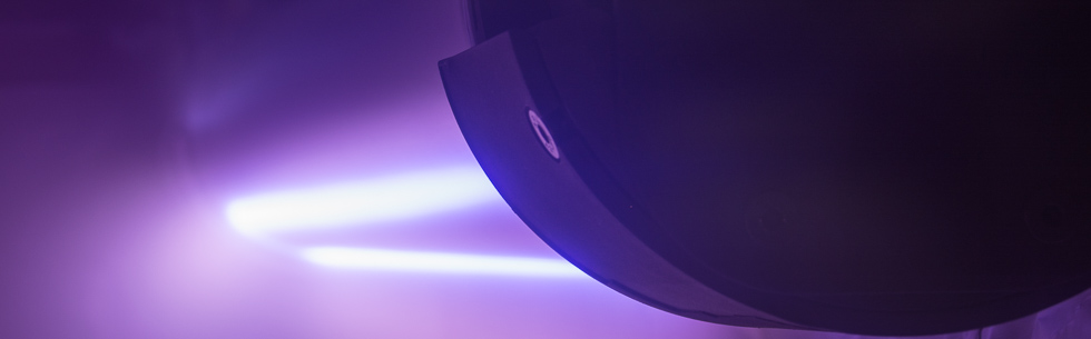
A high negative voltage (-0.5 to -3 kV) is applied to the cathode (usually located behind the sputtering target) and the chamber surrounds act as the anode. Under the correct conditions of pressure and voltage, a plasma is generated as a result of electrons being accelerated away from the cathode leading to collisions with the sputtering gas atoms in the vicinity, to create a cloud of ionized argon gas ions. The associated photon production emits light, hence a plasma typically has a very attractive visual effect.
The positively charged argon ions are attracted to the negatively charged target at a high velocity which ‘sputters’ atomic size particles from the target source material because of the ion impact and momentum transfer to the target surface. The sputtered particles generated are emitted with high kinetic energy and travel across the vacuum space to create a sputter vapour flux. Any surface in contact with this flux of vapour will be coating with the target material. [2]
Since no melting of the source material is required, the sputtering process can operate in any orientation (top, bottom, side), and complex shapes can be coated.
The Principle of Magnetron Sputtering
Magnetron sputtering is a technique that was developed in the 1970s, boasting high speed, low damage, and lower temperature sputtering. It involves the addition of a closed magnetic field over the target surface to enhance the efficiency of the plasma generation by increasing the probability of collisions between electrons and argon atoms close to the target surface. Once the initial collision cascade is established within the magnetic trap, large amounts of ‘secondary’ electrons are generated which further boost the plasma production and density. [3]
The magnetron enhancement creates a lower voltage, higher current discharge compared to the standard sputtering method. The higher density of ionized species creates a much more rapid sputtering of the target material, and hence is a higher rate coating process. Modern power supplies used to create and sustain such discharges have a high degree of stability and control, which means the plasma and coating process is easy to regulate as well as easily scaled to very large size (several m in length).
Applications of Magnetron Sputtering
Magnetron sputter sources are very widely used in a number of industries to deposit very thin coatings onto surfaces. Sputtered coatings are generally just 0.1 µm - 5 µm in thickness and perform a range of functional tasks. Magnetron sputtering is an expensive method to coat surfaces due to its reliance upon a high-quality vacuum environment – vacuum chamber and pumps. It is therefore more costly compared to atmospheric coating, painting /spraying. However, it is simply not possible to create certain materials, thin films and devices without sputtering, so it enjoys a very wide market appeal.
The main examples where magnetron sputtering is applied include the following:
- Thin film solar cells
- Semiconductor chips and microelectronic packaging
- Anti-reflective and anti-static layers on visual displays – TFT, LCD, OLED, CRT
- Thin film batteries
- LED type lighting – large area ‘light’ surfaces
- Touch screen layers on displays – dielectric and TCO
- Barrier layers for OLED, LED, Solar cells, thin film batteries.
- Solar control coatings on architectural glass
- Wear resistant coatings on machine cutting Tools
- Low friction coatings on machine & engine Parts
Find Out More
To find out more about magnetron sputtering and its uses, visit Gencoa’s dedicated webpage here.
References
1. https://angstromengineering.com/tech/magnetron-sputtering/
2. http://www.semicore.com/what-is-sputtering
3. https://www.intechopen.com/online-first/63559
Contact Gencoa

To contact Gencoa at our Liverpool headquarters, click for contact details.
For details of international representatives, refer to our list of worldwide contacts.